
 National and Kapodistrian University of Athens
Semiconductor and Microsystems Laboratory
National and Kapodistrian University of Athens
Semiconductor and Microsystems Laboratory
 Solid State Physics Section
Department of Solid State Physics
Solid State Physics Section
Department of Solid State Physics
 Department of Solid State Physics, Faculty of Physics, University of Athens
University of Athens, School of Science, Faculty of Physics, Department of Solid State Physics, Contact, Maps
Penepistimiopolis Zografos, Athens 15784 | Phone: +30 210 7276-722 | Fax: +30 210 7276-711
Department of Solid State Physics, Faculty of Physics, University of Athens
University of Athens, School of Science, Faculty of Physics, Department of Solid State Physics, Contact, Maps
Penepistimiopolis Zografos, Athens 15784 | Phone: +30 210 7276-722 | Fax: +30 210 7276-711


 Semiconducting
Materials
Semiconductor
Devices
MEMS
Nanocomposites
Reliability
Materials and
Transport parameters
Point defects
Dielectric films
Micro-Electro-Mechanical System Switches (MEMS)
Device research
The research activity focuses mainly on the issue of
dielectric charging in Micro-Electro-Mechanical System
(MEMS) capacitive switches. The charging is investigated:
(i) in devices with a wide range of dielectric materials such
as
* Si3N4 and SiO2 deposited under different conditions, such
as temperature, PECVD frequency and gas flow ratios
* AlN and Al2O3
* nanostructured dielectrics such as:
- nanocrystalline diamond,
- TiO2 and
- Si3N4 with embeded nanoparticles
(ii) in floating electrode devices
(iii) on the effect of field emission, in devices being in up-
state with and without dielectric film, and its impact on
dielectric charging
(vi) with moving armature in down-state (contacted
charging) and up-state (contact-less charging)
The research activities also include:
* the impact of the presence of a floating electrode
and the condition of pull-in state, when activation is
performed through the transmission line, is also
investigated
* the actuation in dielectric-less and pillar-less
devices
* the calculation of discharge current through the
dielectric film
The parameters tested are:
* Capacitance - Voltage characteristics in vacuum
and temperature range of 100K to 450K
* Capacitance - Voltage characteristics in different
gas ambient and temperature range of 300K to 450K
* Measurement of dielectric film surface potential by
applying the Kelvin Probe model
* Direct measurement of dielectric film surface potential
decay with Kelvin Probe setup
* Direct measurement of top electrode potential decay
with Kelvin Probe setup
* Lifetime test through cycling under different stress
bias, switching frequencies and duty cycles
* All assessment are performed in the temperature
range of 100 K to 450 K under vacuum or 300K to 450K
under controlled environment such as nitrogen,
controlled humidity etc.
next
Semiconducting
Materials
Semiconductor
Devices
MEMS
Nanocomposites
Reliability
Materials and
Transport parameters
Point defects
Dielectric films
Micro-Electro-Mechanical System Switches (MEMS)
Device research
The research activity focuses mainly on the issue of
dielectric charging in Micro-Electro-Mechanical System
(MEMS) capacitive switches. The charging is investigated:
(i) in devices with a wide range of dielectric materials such
as
* Si3N4 and SiO2 deposited under different conditions, such
as temperature, PECVD frequency and gas flow ratios
* AlN and Al2O3
* nanostructured dielectrics such as:
- nanocrystalline diamond,
- TiO2 and
- Si3N4 with embeded nanoparticles
(ii) in floating electrode devices
(iii) on the effect of field emission, in devices being in up-
state with and without dielectric film, and its impact on
dielectric charging
(vi) with moving armature in down-state (contacted
charging) and up-state (contact-less charging)
The research activities also include:
* the impact of the presence of a floating electrode
and the condition of pull-in state, when activation is
performed through the transmission line, is also
investigated
* the actuation in dielectric-less and pillar-less
devices
* the calculation of discharge current through the
dielectric film
The parameters tested are:
* Capacitance - Voltage characteristics in vacuum
and temperature range of 100K to 450K
* Capacitance - Voltage characteristics in different
gas ambient and temperature range of 300K to 450K
* Measurement of dielectric film surface potential by
applying the Kelvin Probe model
* Direct measurement of dielectric film surface potential
decay with Kelvin Probe setup
* Direct measurement of top electrode potential decay
with Kelvin Probe setup
* Lifetime test through cycling under different stress
bias, switching frequencies and duty cycles
* All assessment are performed in the temperature
range of 100 K to 450 K under vacuum or 300K to 450K
under controlled environment such as nitrogen,
controlled humidity etc.
next
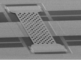
 MEMS capacitive switch
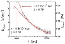
 Discharge current thrugh the dielectric
film in a MEMS capacitive switch
Discharge current thrugh the dielectric
film in a MEMS capacitive switch
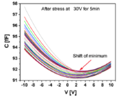
 Shift of bias for capacitance
minimum in up-state resulting
from dielectric film discharge
Shift of bias for capacitance
minimum in up-state resulting
from dielectric film discharge
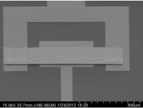
 Structure for field emission studies
in MEMS
Structure for field emission studies
in MEMS