

 National and Kapodistrian University of Athens
Semiconductor and Microsystems Laboratory
National and Kapodistrian University of Athens
Semiconductor and Microsystems Laboratory
 Solid State Physics Section
Department of Solid State Physics
Solid State Physics Section
Department of Solid State Physics
 Department of Solid State Physics, Faculty of Physics, University of Athens
University of Athens, School of Science, Faculty of Physics, Department of Solid State Physics, Contact, Maps
Penepistimiopolis Zografos, Athens 15784 | Phone: +30 210 7276-722 | Fax: +30 210 7276-711
Department of Solid State Physics, Faculty of Physics, University of Athens
University of Athens, School of Science, Faculty of Physics, Department of Solid State Physics, Contact, Maps
Penepistimiopolis Zografos, Athens 15784 | Phone: +30 210 7276-722 | Fax: +30 210 7276-711


 Semiconducting
Materials
Semiconductor
Devices
MEMS
Nanocomposites
Reliability
Materials and
Transport parameters
Point defects
Dielectric films
Semiconductor devices
Device research
Aim of this activity is to investigate the electrical proper-ties
of semiconductor devices. The research is focused on:
* Silicon On Insulator (SOI) MOSFETs
* Thin Film Transistors fabricated on polycrystalline Si
* 2-D and 3-D electron gas devices based on III-V and III-
N semiconductors
The parameters tested are:
* Current-Voltage characteristics above and below
thresshold
* gm dispersion
* Distribution of point and interface defects with the aid of
drain current transient spectroscopy (DLTS and PICTS)
* Backgating effect and substrate current
* Optoelectronic properties in the range of 190 nm to 3200 nm
* Optical backgating dependence on illumination wavelength
and intensity
* Drain current noise spectrum
* All assessment performed in the temperature range of 20 K to
330 K or 90 K to 450 K
Experimental setup
The experimental setup consists of:
* SR785 signal analyser with SR570 low noise current amplifier
for drain current noise measurements
* Keithley 6485, 6487 and 6517A pico-Amperemeters for the
current-voltage characterization
* Device test fixture with DIL-28 zero force socket on PTFE base
for high isolation. Packaged devices are access with 4 triax, two
floating and 2 grounded BNC sockets.
* PAR 124 Lock-In Amplifier, 0.2 Hz to 200 KHz, for
transconductance dispersion and AC impedance
assessment
* Oriel 12.5 cm focal length monochromator with
gratings and filters to cover the range of 190 nm to
3200 nm for optoelectronic properties assessemnt.
* I-DLTS setup
* Probe station with Cascade micromanipulators in
dark box for on wafer assessment
* Cascade Microtech RF-1 probe station with Pico-
Probe CPW probes
* Aeroflex 2397 spectrum analyser with tracking
generator,
* HP bias-T networks
* Return-loss bridges for rf-assessment up to 3 GHz.
* All measurements are computer controlled with
Labview software.
Semiconducting
Materials
Semiconductor
Devices
MEMS
Nanocomposites
Reliability
Materials and
Transport parameters
Point defects
Dielectric films
Semiconductor devices
Device research
Aim of this activity is to investigate the electrical proper-ties
of semiconductor devices. The research is focused on:
* Silicon On Insulator (SOI) MOSFETs
* Thin Film Transistors fabricated on polycrystalline Si
* 2-D and 3-D electron gas devices based on III-V and III-
N semiconductors
The parameters tested are:
* Current-Voltage characteristics above and below
thresshold
* gm dispersion
* Distribution of point and interface defects with the aid of
drain current transient spectroscopy (DLTS and PICTS)
* Backgating effect and substrate current
* Optoelectronic properties in the range of 190 nm to 3200 nm
* Optical backgating dependence on illumination wavelength
and intensity
* Drain current noise spectrum
* All assessment performed in the temperature range of 20 K to
330 K or 90 K to 450 K
Experimental setup
The experimental setup consists of:
* SR785 signal analyser with SR570 low noise current amplifier
for drain current noise measurements
* Keithley 6485, 6487 and 6517A pico-Amperemeters for the
current-voltage characterization
* Device test fixture with DIL-28 zero force socket on PTFE base
for high isolation. Packaged devices are access with 4 triax, two
floating and 2 grounded BNC sockets.
* PAR 124 Lock-In Amplifier, 0.2 Hz to 200 KHz, for
transconductance dispersion and AC impedance
assessment
* Oriel 12.5 cm focal length monochromator with
gratings and filters to cover the range of 190 nm to
3200 nm for optoelectronic properties assessemnt.
* I-DLTS setup
* Probe station with Cascade micromanipulators in
dark box for on wafer assessment
* Cascade Microtech RF-1 probe station with Pico-
Probe CPW probes
* Aeroflex 2397 spectrum analyser with tracking
generator,
* HP bias-T networks
* Return-loss bridges for rf-assessment up to 3 GHz.
* All measurements are computer controlled with
Labview software.
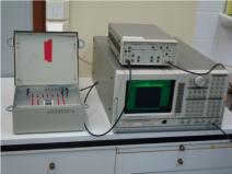
 Signal analyser with current
amplifier and device test fixture
Signal analyser with current
amplifier and device test fixture
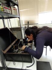
 Probe station with dark box

 Cascade Microtech RF-1
probe station
Cascade Microtech RF-1
probe station