
 National and Kapodistrian University of Athens
Semiconductor and Microsystems Laboratory
National and Kapodistrian University of Athens
Semiconductor and Microsystems Laboratory
 Solid State Physics Section
Department of Solid State Physics
Solid State Physics Section
Department of Solid State Physics
 Department of Solid State Physics, Faculty of Physics, University of Athens
University of Athens, School of Science, Faculty of Physics, Department of Solid State Physics, Contact, Maps
Penepistimiopolis Zografos, Athens 15784 | Phone: +30 210 7276-722 | Fax: +30 210 7276-711
Department of Solid State Physics, Faculty of Physics, University of Athens
University of Athens, School of Science, Faculty of Physics, Department of Solid State Physics, Contact, Maps
Penepistimiopolis Zografos, Athens 15784 | Phone: +30 210 7276-722 | Fax: +30 210 7276-711


 Semiconducting
Materials
Semiconductor
Devices
MEMS
CNT composites
Reliability
Materials and
Transport parameters
Point defects
Dielectric films
Nanocomposites
Material research
Aim of this activity is to investigate
the electrical properties of a wide
range of dielectric materials that
find application in both the
semiconductor devices and MEMS
switches. The dielectric materials
the group investigates are:
* Plasma Enhanced Chemical
Vapor Deposited (PECVD) Silicon Nitride. The
group investigated the impact of deposition
conditions such as plasma frequencey
(13.56MHz, 380KHz or mixed frequency), the
substrate temperature rnaging from 100oC to
350oC, the gas ratio composition etc, since all
these directly affect the material nanostructure.
* PECVD Silicon Nitride with nanostructures
embeded in the host materials
* PECVD Silicon Dioxide
* Nano/micro crystalline diamond
* AlN and Al2O3
* Transition metal oxides such as TiO2, Y2O3,
HfO2, etc
* varius PZT dielectrics
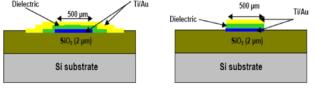
The test structure to assess the dielectric
materials are the Metal-Insulator-Metal (MIM)
capacitors with different geometries. The parameters tested are:
* Current-Voltage characteristics
* Thermally Stimulated Depolarization/Polarization Currents (TSDC/TSPC)
method to investigated point and extended defects
* Charge/Discharge Current Tranient method to monitor the charge/discharge
transients in MIM capacitors
* Capacitance-voltage characteriszation to monitor the exchange of charges with
the dielectric film and the dependence on test signal frequencey
* Kelvin Probe method to monitor the surface potential of dielectric films and/or
the potential of top electrode in MIM capacitors
* All assessment performed in the temperature range of 90 K to 450 K
Experimental setup
The experimental setup consists of:
* TSDC/TSPC setup
* CCT/DCT
* Keithley 6485, 6487 and 6517A pico-Amperemeters for the current-voltage
characterization in MIM capacitors
* Kelvin Probe setup
* Probe station with Cascade micromanipulators in dark box for on wafer
assessment
* Cascade Microtech RF-1 probe station with Pico-Probe CPW probes
* All measurements are computer controlled with Labview software.
Semiconducting
Materials
Semiconductor
Devices
MEMS
CNT composites
Reliability
Materials and
Transport parameters
Point defects
Dielectric films
Nanocomposites
Material research
Aim of this activity is to investigate
the electrical properties of a wide
range of dielectric materials that
find application in both the
semiconductor devices and MEMS
switches. The dielectric materials
the group investigates are:
* Plasma Enhanced Chemical
Vapor Deposited (PECVD) Silicon Nitride. The
group investigated the impact of deposition
conditions such as plasma frequencey
(13.56MHz, 380KHz or mixed frequency), the
substrate temperature rnaging from 100oC to
350oC, the gas ratio composition etc, since all
these directly affect the material nanostructure.
* PECVD Silicon Nitride with nanostructures
embeded in the host materials
* PECVD Silicon Dioxide
* Nano/micro crystalline diamond
* AlN and Al2O3
* Transition metal oxides such as TiO2, Y2O3,
HfO2, etc
* varius PZT dielectrics
The test structure to assess the dielectric
materials are the Metal-Insulator-Metal (MIM)
capacitors with different geometries. The parameters tested are:
* Current-Voltage characteristics
* Thermally Stimulated Depolarization/Polarization Currents (TSDC/TSPC)
method to investigated point and extended defects
* Charge/Discharge Current Tranient method to monitor the charge/discharge
transients in MIM capacitors
* Capacitance-voltage characteriszation to monitor the exchange of charges with
the dielectric film and the dependence on test signal frequencey
* Kelvin Probe method to monitor the surface potential of dielectric films and/or
the potential of top electrode in MIM capacitors
* All assessment performed in the temperature range of 90 K to 450 K
Experimental setup
The experimental setup consists of:
* TSDC/TSPC setup
* CCT/DCT
* Keithley 6485, 6487 and 6517A pico-Amperemeters for the current-voltage
characterization in MIM capacitors
* Kelvin Probe setup
* Probe station with Cascade micromanipulators in dark box for on wafer
assessment
* Cascade Microtech RF-1 probe station with Pico-Probe CPW probes
* All measurements are computer controlled with Labview software.
 MIM capacitors with different geometries
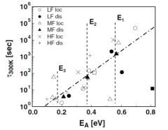
 Distribution of time constants in energy
domain for PECVD Silicon Nitride
Distribution of time constants in energy
domain for PECVD Silicon Nitride