

 National and Kapodistrian University of Athens
Semiconductor and Microsystems Laboratory
National and Kapodistrian University of Athens
Semiconductor and Microsystems Laboratory
 Solid State Physics Section
Department of Solid State Physics
Semiconducting materials
Materials
* Semi-insulating and high resistivity III-V bulk and
epitaxial compound semiconductors
* Low resistivity III-V bulk and epitaxial compound
semiconductors
* Silicon On Insulator (SOI) films
* Thin film polycrystalline Si
* 2-D electron gas heterostructure structures based on III-
V and III-N and dilute nitride semiconductors
* 1-D semiconductors such as [H2CN(I)=NH2]3MI5 etc
* QD layers based on dilute nitride semiconductors
* Silicon and SiGe alloys IR spectroscopy
Transport parameters
The transport properties in semiconducting materials is
assessed by employing the van der Pauw method to
measure the:
* conductivity of bulk material and thin films
* Hall coefficient
* magnetoresistance
* illumination parallel to magnetic field for photoconductivity and
photo-Hall coefficient
and the same and different geometries for:
* illumination normal to magnetic field for magnetophotoele-ctric
effect.
The expermental setup consists of:
* Magnet with field intensity up to 1Tesla
* Closed cycle He APD-Cryogenics cryostat with
temperature controller that allows sample
assessment in the temprature range of 15K to 330K
* Keithley switch matrix (5x4) that allows the
assessment of samples with resistance up to 1012
Ohm
* Keithely 236 SMU for current sourcing and
differential voltage measurement in van der Pauw
geometry
* Vacuum system to ensure accurate tempera-ture
control and electrical measurements at low and high
temperatures
* Oriel monocromator with 12.5 cm focal length
with a set of gratings, band pass filters and
photodetectors to accurately cover the range from
190 nm to 3500 nm.
* All measurements are computer controlled with
Labview software.
Solid State Physics Section
Department of Solid State Physics
Semiconducting materials
Materials
* Semi-insulating and high resistivity III-V bulk and
epitaxial compound semiconductors
* Low resistivity III-V bulk and epitaxial compound
semiconductors
* Silicon On Insulator (SOI) films
* Thin film polycrystalline Si
* 2-D electron gas heterostructure structures based on III-
V and III-N and dilute nitride semiconductors
* 1-D semiconductors such as [H2CN(I)=NH2]3MI5 etc
* QD layers based on dilute nitride semiconductors
* Silicon and SiGe alloys IR spectroscopy
Transport parameters
The transport properties in semiconducting materials is
assessed by employing the van der Pauw method to
measure the:
* conductivity of bulk material and thin films
* Hall coefficient
* magnetoresistance
* illumination parallel to magnetic field for photoconductivity and
photo-Hall coefficient
and the same and different geometries for:
* illumination normal to magnetic field for magnetophotoele-ctric
effect.
The expermental setup consists of:
* Magnet with field intensity up to 1Tesla
* Closed cycle He APD-Cryogenics cryostat with
temperature controller that allows sample
assessment in the temprature range of 15K to 330K
* Keithley switch matrix (5x4) that allows the
assessment of samples with resistance up to 1012
Ohm
* Keithely 236 SMU for current sourcing and
differential voltage measurement in van der Pauw
geometry
* Vacuum system to ensure accurate tempera-ture
control and electrical measurements at low and high
temperatures
* Oriel monocromator with 12.5 cm focal length
with a set of gratings, band pass filters and
photodetectors to accurately cover the range from
190 nm to 3500 nm.
* All measurements are computer controlled with
Labview software.


 Semiconducting
Materials
Semiconductor
Devices
MEMS
Nanocomposites
Semiconducting
Materials
Semiconductor
Devices
MEMS
Nanocomposites


 Department of Solid State Physics, Faculty of Physics, University of Athens
University of Athens, School of Science, Faculty of Physics, Department of Solid State Physics, Contact, Maps
Penepistimiopolis Zografos, Athens 15784 | Phone: +30 210 7276-722 | Fax: +30 210 7276-711
Reliability
Materials and
Transport parameters
Point defects
Dielectric films
Department of Solid State Physics, Faculty of Physics, University of Athens
University of Athens, School of Science, Faculty of Physics, Department of Solid State Physics, Contact, Maps
Penepistimiopolis Zografos, Athens 15784 | Phone: +30 210 7276-722 | Fax: +30 210 7276-711
Reliability
Materials and
Transport parameters
Point defects
Dielectric films
 van der Pauw geometry


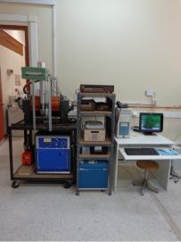 Esperimental setup for assessment of
transport parameters in semiconductors
Esperimental setup for assessment of
transport parameters in semiconductors

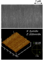
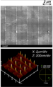 “2N-shot” and “directional”
crystallization
Polycrysytalline Si formed by
excimer-laser annealing crystalli-
zation of amorphous silicon,
using the sequential lateral
solidification (SLS) technique
“2N-shot” and “directional”
crystallization
Polycrysytalline Si formed by
excimer-laser annealing crystalli-
zation of amorphous silicon,
using the sequential lateral
solidification (SLS) technique