Publications
Table of Contents (TOC)
Plasmonic Backscattering Effect in High-Efficient Organic Photovoltaic Devices
Adv. Energ. Mater., 2016, 6 (2), 1501640. DOI: 10.1002/aenm.201501640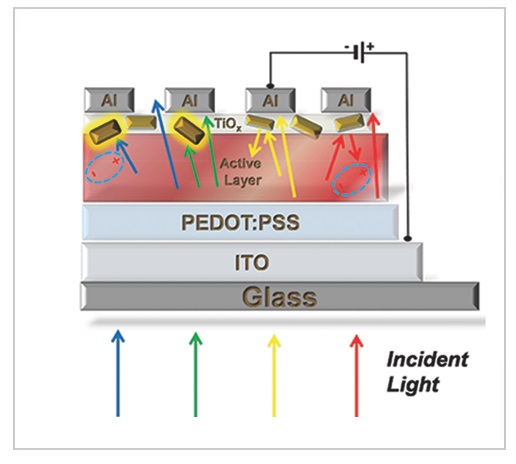
Abstract
A universal strategy for efficient light trapping through the incorporation of gold nanorods on the electron transport layer (rear) of organic photovoltaic devices is demonstrated. Utilizing the photons that are transmitted through the active layer of a bulk heterojunction photovoltaic device and would otherwise be lost, a significant enhancement in power conversion efficiency (PCE) of (PCDTBT:PC71BM) and (PTB7):PC71BM by 13% and 8%, respectively, is observed. PCEs over 8% are reported for devices based on the PTB7:PC71BM blend. A comprehensive optical and electrical characterization of our devices to clarify the influence of gold nanorods on exciton generation, dissociation, charge recombination, and transport inside the thin film devices is performed. By correlating the experimental data with detailed numerical simulations, the near-field and far-field scattering effects are separated for gold nanorods (Au NRs), and part of the performance enhancement is confidently attributed to the enhanced absorption caused by backscattering. While a secondary contribution from the Au NRs that partially protrude inside the active layer and exhibit strong near-fields due to localized surface plasmon resonance effects is also observed, it is minor in magnitude. Furthermore, another important contribution to the enhanced performance is electrical in nature and comes from the increased charge collection probability.
For citation:
Kakavelakis, G.; Vangelidis, I.; Heuer-Jungemann, A.; Kanaras, A. G.; Lidorikis, E.; Stratakis, E.; Kymakis, E.
"Plasmonic Backscattering Effect in High-Efficient Organic Photovoltaic Devices"
Adv. Energ. Mater. 2016, 6 (2), 1501640. DOI: 10.1002/aenm.201501640